Characterization of a Superconducting NbSi Transition Edge Sensor for TeSIA
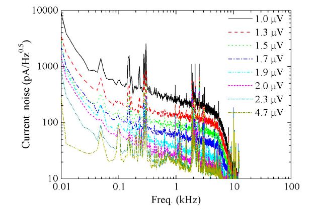
Our superconducting TES device is based on NbSi film, which is co-evaporated on the top of a SiO/SiN/SiO trilayer on a Si substrate. Thermometers are patterned and plasma etched in a fluorine-based mixture. Niobium contacts are evaporated and covered with gold pads to allow wire-bonding. Finally the silicon wafer is completely etched by a deep reactive ion etching. We firstly measured the current-voltage characteristics at different bath temperatures from 288 mK to 440 mK, from which the thermal conductance between TES device and substrate is derived to be 345 pW/K. We then measured the current noise at different bias voltages along the I-V curve at 288 mK. The noise equivalent power (NEP) within the transition is about 8x10-17W/√Hz, which is already less than the specification of the TeSIA. An 8x3 TDM readout scheme based on SQUIDs and an ASIC is under development. Preliminary test results show that the ASIC works well at room temperature. A large TES array with background limited sensitivity is suitable for ground-based application at Dome A, Antarctica. The work by W. Zhang, J. Q. Zhong, W. Miao, W.Y. Duan, Q. J. Yao, S. C. Shi (corresponding author), J. Martino, F. Pajot, D. Prele, F. Voisin, and M. Piat, accepted by IEEE Transactions on applied superconductivity, has been published online ( http://ieeexplore.ieee.org/stamp/stamp.jsp?arnumber=6930745).